
How Innovative Techniques Are Revolutionizing Flex PCB Fabrication
 anyejohnson
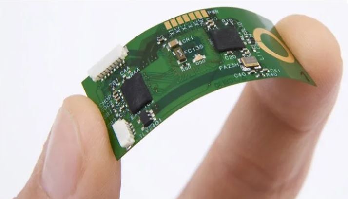
Flexible printed circuit boards (flex PCBs) have become an integral part of modern electronics due to their lightweight, flexible, and compact nature. Used in applications ranging from consumer electronics to medical devices and automotive systems, flex PCBs offer design flexibility and performance benefits that rigid PCBs can’t match. As the demand for smaller, more versatile electronics grows, so does the need for more efficient, reliable, and advanced manufacturing processes in flex PCB fabrication.
In recent years, innovative techniques and technologies have emerged that are revolutionizing the flex PCB fabrication service landscape. These innovations not only improve the efficiency and reliability of the production process but also enhance the overall performance and durability of flex PCBs. This article explores some of the latest advancements in flex PCB fabrication that are shaping the future of electronics design.
High-Density Interconnect (HDI) Technology
High-Density Interconnect (HDI) technology has become a critical innovation in flex PCB fabrication. As electronic devices become smaller and more complex, the need for compact circuit designs increases. HDI enables the creation of PCBs with a higher wiring density by using thinner traces and smaller vias. This technology allows designers to pack more components into a smaller area, making it possible to develop more complex, multi-layer circuits on flexible substrates.
By incorporating microvias, blind and buried vias, and fine-line routing, HDI significantly improves signal integrity and performance. This is particularly useful in applications like smartphones, wearable devices, and medical equipment, where space constraints are critical. HDI technology allows flex PCBs to maintain their mechanical flexibility while supporting the intricate circuitry required in advanced devices.
Advanced Materials for Flexibility and Durability
Material innovation is at the core of advancements in flex PCB fabrication. Traditional rigid PCBs use materials like FR4, which offer excellent durability but lack the flexibility needed for dynamic applications. In contrast, modern flex PCBs utilize advanced materials such as polyimide, which offers both flexibility and high thermal stability.
Polyimide is widely used due to its ability to withstand high temperatures, making it ideal for high-frequency applications or environments where thermal cycling is frequent. Additionally, flexible materials like liquid crystal polymer (LCP) are becoming increasingly popular in flex PCB fabrication due to their superior electrical properties and resistance to moisture, heat, and chemicals. These materials not only extend the lifespan of flex PCBs but also improve signal integrity and reduce the risk of failure in demanding applications.
Innovative material combinations are also leading to the development of hybrid flex-rigid PCBs, which integrate both flexible and rigid sections within a single design. This allows designers to harness the benefits of both flexibility and rigidity, offering greater design freedom and enhanced reliability.
Additive Manufacturing and 3D Printing
Additive manufacturing, including 3D printing, has made significant strides in recent years and is now being applied to flex PCB fabrication. Traditional PCB manufacturing involves subtractive processes, where material is etched away to create the circuit patterns. In contrast, additive manufacturing builds up the circuit layer by layer, offering more precision and reducing material waste.
3D printing in flex PCB fabrication allows for more intricate designs, as it can deposit conductive materials onto flexible substrates with high accuracy. This technique opens up new possibilities for custom shapes, complex geometries, and multi-layer circuits. Additive manufacturing also speeds up the prototyping process, allowing for rapid iterations and quicker time-to-market for new products.
The ability to 3D print flex PCBs with embedded components and interconnections is another exciting development. This eliminates the need for soldering, further improving the durability and reliability of the PCB. As 3D printing technologies advance, they are expected to play a significant role in the future of flex PCB fabrication services.
Laser Direct Imaging (LDI) for Precision and Accuracy
Laser Direct Imaging (LDI) is an advanced technique that uses lasers to expose the circuit pattern directly onto the flexible substrate, replacing traditional photolithography methods. LDI is revolutionizing flex PCB fabrication by improving accuracy and enabling the creation of finer, more complex circuit patterns.
One of the main advantages of LDI is its ability to achieve high-resolution imaging, making it possible to produce precise circuit layouts with tighter tolerances. This is essential for the miniaturization of electronics, where even the smallest misalignment can affect performance. LDI also eliminates the need for photomasks, reducing production time and costs.
In addition, LDI allows for more flexible designs, as it can image curved or uneven surfaces. This opens up new possibilities for applications where traditional flat PCBs are not suitable, such as in wearables or medical devices that need to conform to the human body.
Automated Optical Inspection (AOI) and Quality Control
As flex PCBs become more complex and miniaturized, ensuring their quality and reliability is more challenging. Automated Optical Inspection (AOI) systems have emerged as a key innovation in the quality control process for flex PCB fabrication services. AOI uses high-resolution cameras and image processing software to inspect the PCB for defects such as misalignments, missing components, or electrical shorts.
The integration of AOI systems in flex PCB fabrication allows for real-time monitoring and ensures that any defects are identified early in the production process. This significantly reduces the risk of faulty products reaching the market, improving overall reliability and customer satisfaction.
In addition to AOI, other advanced inspection techniques like X-ray inspection and Automated Test Equipment (ATE) are being used to verify the integrity of flex PCBs. These methods ensure that the circuits function as intended and can withstand the stresses of real-world applications.
Improved Flex-to-Install Designs
One of the key challenges in flex PCB design is ensuring that the circuit can withstand repeated flexing without failing. Traditional flex PCBs were often designed to bend during installation but remained static during operation. However, with the growing use of flexible electronics in dynamic applications—such as in wearables, robotics, and aerospace—there is an increasing need for flex PCBs that can endure continuous bending and movement.
Innovative design techniques, such as flex-to-install and dynamic flex designs, are being implemented to improve the mechanical reliability of these circuits. Flex-to-install designs ensure that the PCB can be bent or folded during installation without damaging the circuit, while dynamic flex designs allow for continuous bending during operation. These advancements are essential for applications like robotics and medical devices, where mechanical flexibility is crucial for proper functionality.
Environmental and Sustainable Practices in Flex PCB Fabrication
As the world moves towards more sustainable manufacturing practices, the flex PCB fabrication service industry is also embracing eco-friendly innovations. One of the significant developments is the use of lead-free materials and environmentally friendly manufacturing processes, which reduce the environmental impact of production.
Innovations such as water-based cleaning processes and reduced use of hazardous chemicals in PCB fabrication are gaining traction. Additionally, new recycling techniques for discarded or outdated PCBs are being developed to minimize electronic waste, contributing to a more sustainable future for the electronics industry.
Conclusion
The evolution of flex PCB fabrication services is being driven by a combination of material innovations, advanced manufacturing techniques, and automation technologies. From High-Density Interconnect (HDI) technology to 3D printing and Laser Direct Imaging (LDI), these cutting-edge techniques are revolutionizing how flex PCBs are designed and manufactured.
As the demand for smaller, more flexible, and durable electronics continues to grow, these innovations will play a crucial role in shaping the future of electronics. The ability to integrate advanced materials, improve precision, and enhance reliability ensures that flex PCB fabrication services remain at the forefront of technological progress.
By incorporating these latest techniques, flex PCB manufacturers can offer enhanced solutions that cater to the increasingly complex requirements of modern electronics, providing companies with the tools they need to stay ahead in an ever-evolving industry. As technology continues to advance, the future of flex PCB fabrication promises even more exciting developments, pushing the boundaries of what’s possible in electronic circuit design.